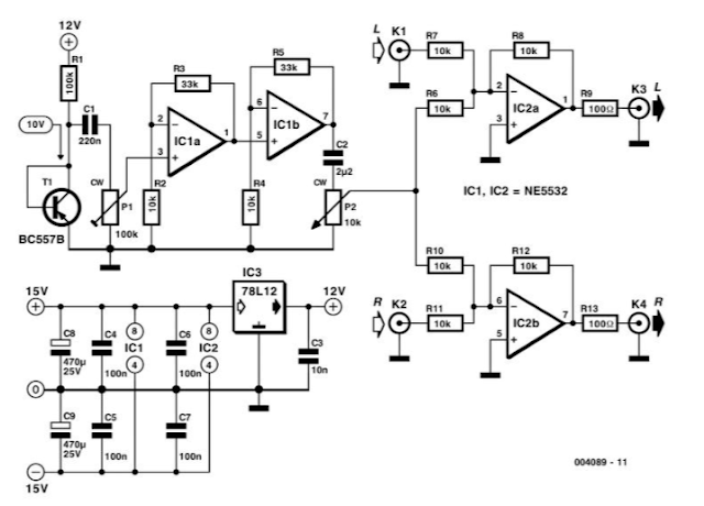
This Circuit is primarily intended to be used by persons who want to experiment with audio. For example, you can determine whether your own audible threshold for noise is different with and without music, or whether a particular CD sounds better with a little bit of noise. However, since this circuit produces white noise, it can also be used for test measurements, such as comparing the sounds of different loudspeakers, measuring filter characteristics and so on. The measured characteristics, as shown in Figure 2, show a nearly flat amplitude distribution (averaged over 64 measurements). The effective value of the noise signal at the output is around 100 mV maximum (with both potentiometers set to maximum), measured over the frequency range of 22 Hz to 22 kHz.
The noise is generated by reverse-biasing the base-emitter junction of a PNP transistor (BC557B) so that it zeners. In our prototype, the voltage across Tl was approximately 10 V. PI is used to set the level of the generated noise so that it is just audible, following which the output level can be adjusted using the logarithmic potentiometer P2. For making measurements, PI can also be simply set to its maximum position. The noise is amplified by two opamp stages. Depending on the transistor manufacturer, or the type of transistor if you use a different type, the level of the generated noise can vary significantly. Using two amplification stages in series provides more options and considerably more bandwidth, and you can implement various filter characteristics around ICla and IClb according to your own taste. The gain of the two stages has been kept equal to ensure the maximum possible bandwidth. The amplified signal is then passed to a simple summing amplifier (IC2). We have used a stereo arrangement, in which both channels receive the same noise signal. If you want to expand on the design, you can provide each channel with its own noise generator. In this case, you will have to use a dual potentiometer for P2.
The well-known NE5532 is used for the amplifiers, but any other good dual opamp would also be satisfactory. The opamps are fed from a standard, symmetrical ±15-V supply. In order to suppress possible positive feedback via the power supply, and to reduce the effects of power supply noise (since the opamps are non-inverting), the supply for the noise diode circuit (Rl and Tl) is separately stabilised by IC3 (7812) and extra filtering for the ± 15-V supply is provided by C8 and C9. IC3 must be located as close as possible to Rl, Tl and IC1. The coupling capacitors CI and C2 are necessary to prevent the DC component of the noise signal from appearing at the outputs.
The table lists some measured characteristics of the circuit, for a bandwidth B of 22 Hz to 22 kHz and a reference level of 2V eff .


No comments:
Post a Comment