Antenna Handbook | Best Antennas, Antenna Free Calculators & Top Antenna Deals

3 Pole Bandpass Filter for uhf digital tv 470-800 MHz


This 3 pole bandpass filter using https://wetnet.net/rf_design/3pole.main.cgi  design calculator online.
this bandpass filter is butterworth filter and intended to filter digital tv bandwith 470MHz to 800 MHz , and only this signal will detected after antenna.
Parameter of filter :
Band Frequency 470 - 800 MHz
Center Frequency = 635 MHz
Bandwith = 400 MHz
Impedance = 50 ohm

Input this parameter to online filter calculator above :

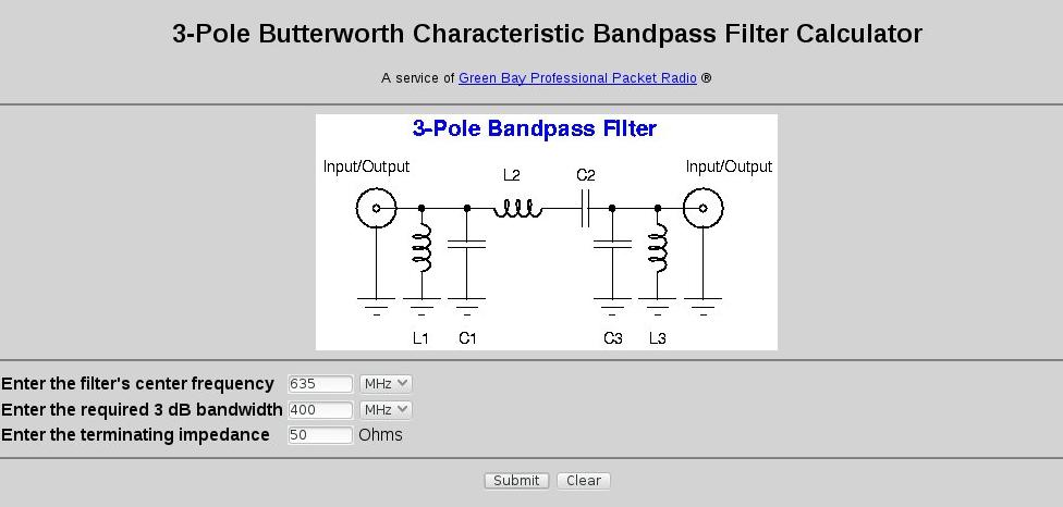
 Click Submit , and the result :


L1,L3 : 0.008763 uH ( 8,763 nH)
L2      : 0.039789 uH (39.789nH)

C1,C3 : 0,000008 uF ( 8 pF)
C2      : 0,000001753 uF (1,753 pF)

We must determine for Inductor L1,L2,L3 the coil diameter, coil length and number of turn of coil.
Using online calculator from  http://www.qsl.net/in3otd/indcalc.html we can determine diameter, length and number of turn coil.
For L1,L3 :

L = 0,00876 uH , coil diameter will be  d : 0,01 m  , Coil length will be l  : 0.01 m and number of turns , n : 1,1355

And for L2 :

L = 0,0396 uH , coil diameter will be d : 0,0259 m , coil length will be l : 0,01 m and number of turns n : 1,1355

The most important thing of build filter is the connection between component should be as close as possible, for avoiding wild capacitance that will generate noise, and the ground area of PCB should be good and wide.
On the next article, I will posting the implementation of this filter.

LSI Chip intel Programmable Peripheral Interface (PPI) 8255

Intel Chip PPI 8255


Image courtesy of wikipedia.org

Chip LSI internal configuration PPI 8255 shows the figure 1. In figure 1, pin IC 8255 consists of 3 groups:
1. Read / Write Control Logic
2. Data Bus Buffer
3. Input / Output Ports

Image courtesy of wikipedia.org


READ / WRITE CONTROL LOGIC

Groups Read / Write Control Logic organize all data and controls, both internal transfers Form and Form of Transfer externally. ACCEPT singer group input from address bus and bus control CPU, the group later realize Ke - Control group. Pin - pin Of The Read / Write Control Logic is as follows:

CS (Chip Select)

Low ON signal pin singer will be to enable communication LSI Chip PPI BETWEEN 8255 TO microcomputers.

RD (Read):
Low ON signal pin singer will be to enable the CPU to review read status information OR Data From Chip LSI PPI 8255

WR (Write)
Low ON signal pin singer will be to enable the CPU to write a review OR Data Into PPI control word 8255
A0 and A1:
The input selector is functioning as part of the Joint Control word - the same WITH RD and WR. Basic Operations The Group is controlled by the Read / Write Control Logic singer portrayed ON the table below.

re:
ON logic high reset input will be to clear the contents of the list of controls and harbor ALL To set the input mode.

Control Group A and Group B:

Configuration functions From EVERY port in the software program by. IN AN basically CPU provides output control word addressed to the LSI Chip Control Word 8255. PPI mode provides information about, bit set, bit reset, And Others. Singer configuration is used to initialize the configuration functions review Chip LSI 8255 PPI.

EVERY Control blocks (Group A and Group B) RECEIVE command From the Read / Write Control Logic, And said menerimacontrol Data From internal bus (internal data bus) and execute commands - Commands Right to review arrangements port - port ITU. ON said control registers can only perform write operations, NO can perform read operations.

DATA BUS BUFFER
The data bus is a 3 state buffer 8 bit With operations Operating prayer Arah (both directions), ayng used to review 8255 WITH connect Chip PPI data bus system. Data Sent and received through the data buffer bus, Similarly to review the control word.

PORT INPUT / Output
Port Input / Output Was Part Of The 8255 PPI chip serves as a liaison

Bandpass filter for uhf television 470-800MHZ

For good reception of uhf tv and digital tv, bandpass filter is a choice for avoiding another signal beside uhf tv channel signal. there are 3 type of bandpass filter that be known , Butterworth, Chebyshev and Bessel filter design.
As shown in this design ,   I am using  http://www.wa4dsy.net/filter/filterdesign.html software online design, or can also using Chebyshev design from http://www.changpuak.ch/electronics/chebyshev_bandpass.php 

Input frequency center for 470-800 MHz, 635 MHz , select bandpass filter or bandstop filter design as menu shown.


after input frequency center, bandwidth of the filter 330 mhz, and the impedance input/output 50 ohms, than select compute parts and the result of filter design will be shown as below.


Build This Digital TV Indoor Antenna 470-800 MHz

I get this idea after searching and studying literature from ARRL handbook, other sources and by experimenting several times. Although my design not perfectly design, but it shows several Channel TV in digital reception with good quality. And several of channels not in good quality. I think the future design of this antenna will give good performance for digital indoor TV antenna.

As mention in ARRL handbook, for high frequency , the equation for finding element length is :

L = 468 / Fo ( in Feet)

Where Fo = Center Frequency

If We design for 470 - 800 MHz , the center frequency will be Fo = 635 MHz, substitute to the equation :

L = 468 / 635 =  0.737 feet , convert to cm . 1 feet = 30.48 cm , so for 0.737 feet equals to :

L = 0.737 feet x 30.48 cm/feet  = 22.46 cm , this is 1/2 lambda for UHF signal in 635 MHZ.

1/4 lambda will be 11.23 cm

As I read in one of literature from S.W. Su and F.S. Chang from Lite On Technology Corporation , Taiwan and Department of Electronics Cheng Shiu University Taiwan. Wideband Rod Dipole Antenna with a modified feed for DTV Signal Reception.
From that literature we can have the design of PCB , feed gap, and dipole design.


I use experiment PCB, and cut the corresponding to the design.The result of antenna as shown .


My design not exactly the same as the design from S.W. Su , i use 1/4 lambda for both arms.

9.3 dBi Yagi TV Antenna 470-800 MHz

I build this Yagi antenna , using material that I have in home. I used boom from stainless steel , with boom length 583 mm. And using copper wire with diameter 1 mm as elements and reflector and driven element. 
For wire length of elements and elements spacing. I used software for Yagi Antenna from K7MEM online Yagi Antenna calculator from Martin E. Meserve. 
Thanks to Martin who has been simplest the process of calculating and designing in Yagi Antenna. Just enter the center frequency of Band frequency we want for antenna to cover, enter boom length  or gain we want to get. Driven element diameter, parasitic element diameter and click the calculate in menu and get the result for Yagi antenna design in another page.

As my design in Yagi antenna, I design for Digital and Analog TV for frequency 470 MHz - 800 MHz Band.
I choose center frequency in 635 MHz.
See the attachment result of my Yagi Antenna design. 


Because my design using Metal Boom Insulated , I used yellow plastic as insulated material and plug in the copper wire to this plastic and tight it with tape plastic.

As seen in picture , I am not yet connect the driven element to balun. The Balun design also calculated with K7MEM calculator in another page.
As seen in design picture, this antenna yagi have gain approximately 9.3 dBi.
My goals on this experiment to make sure that this design works in reality and can received TV signal more good than small antenna I have built later as Indoor antenna. I will publish later. I don't now how much gain this antenna have, but have good reception in several channel and also with no noise in several channel.


I will get back to connect this antenna to balun and connector and will see how the result in this week.