Buil This High Gain Rhombic TV Antenna

This Rhombic Antenna was from Popular Electronics Magazine October 1975 Edition. Cheap cost Antenna , and if your roof house non metallic can match with contour house. Easy to build and Install , provides good reception , almost 14 dB gain. It can be installed without support masts. High gain, broad bandwidth and good directionallity are characteristic of the rhombic's performance.

Rhombic Antenna Design 

 The first step in designing the rhombic is to decide what channels you want to recieve.

The relative location of their transmitting antennas with respect to your home. And the physical layout of the installation site ( we assume the antenna is mounted horizontally on the pitched roof of wood house) , for modern today house we should move antenna to outside of roof, because today house construction using steel frame.

For optimum result three basic designs are given, covering VHF Lo, VHF Hi, and UHF Bands. The VHF Lo Antenna measures 25 Feet ( 7.6 m) on a side and cover channels 2 through 6 and the FM Broadcast Bands.
The VHF Hi design , spanning channels 7 through 13, has legs one-third the length of those for VHF Lo.


Our TV Antenna Type and Specification List we can offer

TV Antenna 
Type : YNX-HD-T-C01


Specification 


Minimal Quote : 100 pcs , maximum Quote : 5000 pcs


TV Antenna 
Type : YNX-HD-T-C02

Specification :


Minimal Quote : 100 pcs , maximum Quote : 5000 pcs


Type TV Antenna
YNX-HD-T-C03


Specification
Minimal Quote : 100 pcs , maximum Quote : 5000 pcs


Type TV Antenna
YNX-HD-T-C04

Specification
Minimal Quote : 100 pcs , maximum Quote : 5000 pcs


Type TV Antenna

YNX-HD-T-C05


Specification


Minimal Quote : 100 pcs , maximum Quote : 5000 pcs


Build The Microcomputer SAP-1 (Continues 1)

As described in article before about the architecture of Microcomputer SAP-1 , in this article we will continue with other part of Microcomputer Diagram Block and circuit .
For you reference , in figure 10-1 as described  have Instruction Register, Accumulator, B Register, Output Register, and Binary Display, We will describe all about it in this article.


Instruction Register

The Instruction register is part of the control unit. to fetch an instruction from the memory the computer does a memory read operation. 

This places the contents of the addressed memory location on the W bus . At the same time, the instruction register is set up for loading on the next positive clock edge.

The contents of the instruction register are split into two nibbles. The upper nibble is a two-state output that goes directly to the block labeled "Controller sequencer". The lowe nibble is a three-state output that is read onto the W bus when needed.

Controller-Sequencer

The lower left block contains the controller-sequencer. Before each computer run, a Low CLR signal is sent to the program counter and a CLR signal to the instruction register.
 

Build The SAP-1 Microcomputer

This articles is from Book of Digital computer electronics : an introduction to microcomputers , book written by Albert Paul Malvino.

The SAP (Simple-As-Possible) computer has been designed for the beginner. The Main Purpose of SAP is to introduce all the crucial ideas behind computer operation without burying you in unnecessary detail. But even a simple computer like SAP covers many advanced concepts. to avoid bombarding you with too much all at once, we will examine three different generations of the SAP computer.

SAP-1 is the first stage in the evolution toward modern computers. Although primitive, SAP-1 is a big step for a beginner. So, dig into SAP-1, master SAP-1, its architecture, its programming , and its circuits, Then you will be ready for SAP-2. 

The Architecture 


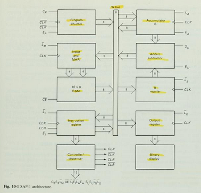
Figure 10-1 shows the (structure) of SAP-1, a bus-organized computer. All register outputs to the W bus are three-state; this allows orderly transfer of data . All other register outputs are two-state; these outputs continuously drive the boxes they are connected to.

The layout of fig. 10-1  emphasizes the registers used in SAP-1. For this reason , no attempt has been made to keep all control circuits in one block called the control unit, all input-output circuits in another block called the I/O unit, etc.

many of registersof Fig. 10-1 are already familiar from earlier examples and discussions. What follows is a brief description of each box; detailed explanations come later.

The Circuit Diagram


Program Counter

The program is stored at the beginning of the memory with the first instruction at binary address 0000, the second instruction at address 0001, the third at address 0010, and so on. The program counter, which is part of the control unit, counts from 0000 to 1111. It is job is to send to the memory the address of the next instruction to be fetched and executed. It does this as follows.

The Program Counter is reset to 0000 before each computer run. When the computer run begins, the program counter sends address 0000 to the memory. The program counter is then incremented to get 0001. After the first instruction is fetched and executed, the program counter sends address 0001 to the memory. Again the program counter is incremented. After the second instruction is fetched and executed, the program counter sends address 0010 to the memory. In this way, the program counter is keeping track of the next instruction to be fetched and executed.

The program counter is like someone pointing a finger at a list of instructions, saying do this first, do this second, do this third, etc. This is why the program counter is sometimes callled a pointer; it points to an address in memory where something important is being stored. 


Input and MAR

Below the program counter is the input and MAR block. It includes the address and data switch registers. These Switch registers, which part of the input unit, allow you to send 4 address bits and 8 data bits to the RAM. As you recall, instruction and data words are written into the RAM before a computer run.

The Memory address register (MAR) is part of the SAP-1 memory. During a computer run, the address in the program counter is latched into the MAR. A bit later, the MAR applies this 4-bit address to the RAM, where a read operation is performed.

The RAM

The RAM is a 16 X 8 static TTL RAM. You can program the RAM by means of the address and data switch registers. This allows you to store a program and data in the memory before a computer run.
During a computer run, the RAM receives 4-bit addresses from MAR (Memory Address Register) and a read operation is performed, In this way , the instruction or data word stored in the RAM is placed on the W bus for use in some other part of the computer. 

On the next article, I will describe  Instruction register, controller sequencer, Accumulator/A Register, Adder/Subtractor, B Register, Output Register, and Binary Display.

What is Filter Circuit ?

filter is a circuit that is capable of passing a specific range of frequencies while block-ing other frequencies. The four major types of filters include low-pass filters, high-pass filters, bandpass filters,and notch filters(or band-reject filters). A low-pass filter passes low-frequency components of an input signal, while a high-pass filter passes high-frequency components. A bandpass filter passes a narrow range of frequencies centered around the filter’s resonant frequency, while a notch filter passes all frequencies except those within a narrow band centered around the filter’s resonant frequency

 Filters have many practical applications in electronics. For example, within a dc power supply, filters can be used to eliminate unwanted high-frequency noise present within the ac line voltage, and they act to flatten out pulsing dc voltages generated by the supply’s rectifier section. 

In radio communications, filters make it possible for a radio receiver to provide the listener with only the desired signal while rejecting all others. 

 Likewise, filters allow a radio transmitter to generate only one signal while attenuating other signals that might interfere with different radio transmitters’ signals. 

In audio electronics, filter networks called crossover networks are usedt o divert low audio signals to woofers, middle-range frequencies to mid range speakers, and high frequencies to tweeters. 

The list of filter applications is extensive.There are two filter types covered in this chapter, namely, passive filter sand active filters. 

Passive filters are designed using passive elements (e.g., resistors, capacitors,and inductors) and are most responsive to frequencies between around 100 Hz and 300 MHz. 

The lower frequency limit results from the fact that at low frequencies the capacitance and inductance values become exceedingly large, meaning prohibitively large components are needed. 

The upper frequency limit results from the fact that at high frequencies parasitic capacitances and inductances wreak havoc.) 

When designing passive filters with very steep attenuation falloff responses, the number of inductor and capacitor sections increases. 

As more sections are added to get the desired response, the greater is the chance for signal loss to occur. Also, source and load impedances must be taken into consideration when designing passive filters. 

Active filters, unlike passive filters, are constructed from op amps, resistors, and capacitors—no inductors are needed. Active filters are capable of handling very low frequency signals (approaching 0 Hz), and they can provide voltage gain if needed(unlike passive filters). 

Active filters can be designed to offer comparable performance to LC filters, and they are typically easier to make, less finicky, and can be designed without the need for large-sized components. 

 Also, with active filters, a desired input and output impedance can be provided that is independent of frequency. One major drawback with active filters is a relatively limited high-frequency range. 

Above around 100 kHz or so, active filters can become unreliable (a result ofthe op amp’s bandwidth and slew-rate requirements). 

At radio frequencies, it is best to use a passive filter

(from Book :  Practical Electronics for Inventors by : Paul Scherz)