Antenna Handbook | Best Antennas, Free Calculators & Top Antenna Deals

Voltage Divider


Voltage Devider: Complete Guide, Formula, Examples, and Applications

Voltage devider is one of the most searched electronics terms by beginners, students, and hobbyists. Although the technically correct term is voltage divider, the principle remains the same: dividing a higher voltage into a lower, usable voltage using simple components.

In this complete guide, you will learn how a voltage devider works, how to calculate it, real-world applications, common mistakes, and best practices.


What Is a Voltage Devider?

A voltage devider is a simple electrical circuit made from two or more resistors connected in series. The output voltage is taken from the junction between resistors, producing a fraction of the input voltage.

This circuit is widely used in:

  • Microcontroller input protection
  • Sensor voltage scaling
  • Audio volume controls
  • Biasing transistors
  • Radio and RF circuits

Basic Voltage Devider Circuit

The simplest voltage devider uses two resistors:

Vin ── R1 ──┬── Vout
            |
           R2
            |
           GND

Where:

  • Vin = Input voltage
  • Vout = Output voltage
  • R1, R2 = Resistor values

Voltage Devider Formula

The standard voltage devider formula is:

Vout = Vin × (R2 / (R1 + R2))

This formula is the foundation of all voltage devider calculations.


Why Voltage Devider Works (Theory)

The voltage devider works because of Ohm’s Law:

V = I × R

In a series circuit, the same current flows through all resistors. The voltage drop across each resistor depends on its resistance value.


Voltage Devider Calculation Examples

Example 1: 12V to 6V

  • Vin = 12V
  • R1 = 10kΩ
  • R2 = 10kΩ

Result:

Vout = 12 × (10k / 20k) = 6V


Example 2: 5V to 3.3V Voltage Devider

  • Vin = 5V
  • R1 = 1.8kΩ
  • R2 = 3.3kΩ

Result:

Vout ≈ 3.24V

This is suitable for most 3.3V microcontrollers.


Voltage Devider with More Than Two Resistors

A voltage devider can use multiple resistors in series. The output voltage is taken from different tap points.

General formula:

Vout = Vin × (Rbelow / Rtotal)

This technique is used in voltage ladders and DAC circuits.


Voltage Devider Using Potentiometer

A potentiometer is an adjustable voltage devider.

Common applications include:

  • Audio volume control
  • Brightness control
  • Adjustable reference voltage

Load Effect in Voltage Devider (Very Important)

The most common mistake is ignoring the load effect.

When a load is connected to the output:

  • The output voltage drops
  • The divider ratio changes
  • The circuit becomes inaccurate

Rule of thumb: Load resistance should be at least 10× higher than R2.


Voltage Devider vs Voltage Regulator

Feature Voltage Devider Voltage Regulator
Efficiency Low High
Load Handling Poor Excellent

Power Dissipation in Voltage Devider

Power dissipation in resistors must be calculated:

P = I² × R

Always check resistor power ratings, especially in high-voltage circuits.


Voltage Devider in AC Circuits

Voltage deiders also work in AC circuits using:

  • Capacitors
  • Inductors

These are commonly used in RF, audio filters, and signal conditioning.


Common Voltage Devider Mistakes

  • Using it as a power supply
  • Ignoring load resistance
  • Wrong resistor values
  • No noise filtering

Best Practices for Voltage Devider Design

  • Use resistor values between 1kΩ – 100kΩ
  • Use 1% tolerance resistors
  • Add bypass capacitor for noise
  • Simulate before building

Conclusion

The voltage devider is a fundamental electronics concept that every engineer and hobbyist must understand. While simple, it plays a critical role in signal conditioning, measurement, and control circuits.

Used correctly, a voltage devider is reliable, accurate, and extremely useful. Used incorrectly, it can cause unstable voltages and damaged components.

Master the voltage devider, and you master the foundation of electronics.


Keywords: voltage devider, voltage divider formula, voltage devider circuit, voltage devider calculator, voltage devider examples

VHF Test Transmitter


If you want to be independent of the local radio stations for testing VHF receivers, you need a frequency modulated oscillator that covers the range of 89.5 to 108 MHz — but building such an oscillator using discrete components is not that easy. Maxim now has available a series of five integrated oscillator building blocks in the MAX260x series (see the May 2001 issue of Elektor Electronics), which cover the frequency range between 45 and 650 MHz. The only other thing you need is a suitable external coil, dimensioned for the midrange frequency. The MAX2606 covers the VHF band, although the frequency can only be varied by approximately ±3 MHz around the midrange frequency set by the coil L. The inductance values shown in the table can serve as starting points for further experimenting.The SMD coils of the Stettner 5503 series are suitable for such oscillators. In Germany, they are available from Bürklin (Buerklin.comwith values between 12 nH and 1200 nH. You can thus directly put together any desired value using two suitable coils. If you want to wind your own coils, try using 8 to 14 turns of 0.5-mm diameter silver-plated copper wire on a 5-mm mandrel. You can make fine adjustments to the inductance of the coil by slightly spreading or compressing the coil. The circuit draws power from a 9-V battery. The BC238C stabilises the voltage to approximately 4 V. Although the MAX2606 can work with a supply voltage between +2.7 V and +5.5 V, a stabilised voltage improves the frequency stability of the free-running oscillator. The supply voltage connection Vcc (pin 5) and the TUNE voltage (pin 3) must be decoupled by 1-nF capacitors located as close as possible to the IC pins. The tuning voltage TUNE on pin 3 may lie between +0.4 V and +2.4 V. A symmetric output is provided by the OUT+ and OUT– pins. In the simplest case, the output can be used in a single-ended configuration. Pull-up resistors are connected to each of the outputs for this purpose. You can use a capacitor to tap off the radio signal from either one of
these resistors. Several milliwatts of power are available. At the audio input, a signal amplitude of 10 to 20 mV is enough to generate the standard VHF frequency deviation of ±40 kHz.

Opentherm Monitor Circuit


If you say that the term ‘Opentherm’ is unfamiliar to you, then this will not surprise us the least. Opentherm is a protocol, which can control central heating boilers and hot water systems digitally. ‘Open’ indicates that it is not specific to a single brand. Anyone can, in principle, make use of this protocol, provided you are prepared to hand over several thousand pounds for ‘membership’ and are prepared to keep the information secret (talk about ‘open’…). As a consequence we unfortunately do not know a great
deal about it, but we do have a few technically interesting pieces of information we would like to share with you.

The connection between the master device (usually the room thermostat) and the slave (typically the central heating boiler) consists of two wires, which permits the use of existing cabling. Via this cable the boiler powers the thermostat with DC. In order to prevent wiring errors, the thermostat is fitted with a bridge rectifier, allowing the conductors (positive and negative) to be reversed. The installer cannot make any mistakes here. The master places on this connection a digital signal. Every second, 32-bits are transmitted in Manchester-code and after about 0.2 seconds the slave responds with the return message. Every bit lasts 1 ms,
and a message consists of:

1 Start bit (logical zero)
1 Parity bit
3 Message type
4 Spare
8 Data ID
16 Data
1 Stop bit (logic zero)


From the electrical perspective, an interesting solution has been selected. The boiler sources current, a logic Low is a current between 5 and 9 mA, a logic High a current between 17 and 23 mA. This way the thermostat is always powered. In the opposite direction, the thermostat signals by pulling down the open circuit boiler voltage of 24 V to a voltage less than 9 V (logic Low) or between 15 and 18 V for a logic High. 

So, at the risk of over-emphasising: the boiler provides information by modulating the current, and the thermostat by changing the voltage. All this can easily be observed on an oscilloscope. In order to follow the activities, we have designed a circuit that does not unduly influence the operation, although it causes an unavoidably small voltage drop of course. The boiler is connected to K1; the polarity is of no consequence  because the connector is followed by a bridge rectifier (D1- D4). The thermostat is connected to K2. R4 and IC1a look if the current corresponds with a logic ‘Low’ or a ‘High’ and signal this, electrically isolated, to the DCD of the serial input of your computer. The voltage of the connection is
monitored by R6, R7 and IC1b and copied to DSR. An oscilloscope connected to these points easily shows you the messages going back and forth. It is likely that the current channel shows both messages. When the voltage on the wires changes, there is also an inevitable change in current because the thermostat is a capacitive load. The circuit is powered from the RTS and DSR hand
shaking lines. They have to be made logic Low first, of course. Naturally, it is also possible to connect a power supply of around 10 to 12 V behind the diodes. Those who are keen can write a program to read the serial inputs and decode the Manchester-code to data. Certain information, such as room and boiler temperature can easily be found. Unfortunately we do not have any more information and neither do we have a program. Every now and then there is something to be found in the Internet, so it may be sensible to keep an eye this.

source : Elektor Circuit Collections 2000-2014

Three Component Oscillator


At first glance, this circuit appears to be just a primitive microphone amplifier. Why then is the title of this article
‘Three-component Oscillator’? The answer is very simple:
the microphone is not intended to pick up speech; instead, it is placed so close to the loudspeaker that massive positive feedback occurs. Here we intentionally exploit an effect that is assiduously avoided in public-address systems — the positive feedback results in a terribly loud whistle. The loudspeaker is connected directly to the 12-V supply voltage and the power transistor, so it must be able to handle a power of at least 1.5 W, and it should have an impedance of 8 to 16 Ω. An outstanding candidate can be cannibalised
from an old television set or discarded speaker box. The microphone should be a carbon-powder type from an old-fashioned telephone handset. If you place a switch in series with the power supply, this sound generator can also be used as an effective doorbell or siren. Surprisingly enough, the circuit can also be used as a simple microphone amplifier — hardly hi-fi, of course, but still usable.

source : P. Lay - Elektor Circuit Collections 

2.5-GHz Signal Source


More and more communications systems are operating in the 2.4-GHz ISM (Industrial, Scientific and Medical) band, including Blue
tooth, various WLAN (Wireless Local Area Network) and Home-RF systems. A simple test oscillator for the frequency band between 2.4 GHz and 2.5 GHz can prove useful in testing receivers. Such an oscillator is available from Maxim (www.maxim-ic.com) as a single IC. The MAX2750 covers the frequency range between 2,4 GHz and 2.5 GHz using in internal LC network that can be tuned using a varactor diode that is also built into the IC. An output buffer delivers a level of –3 dBm into 50 Ω.
This component is housed in an 8-pin µMAX package. The circuit is powered from a 9-V battery. The BC238C transistor stabilises the battery voltage at around 4 V. Although the MAX2750 can work with supply voltages
between +2.7 V and +5.5 V, the frequency stability of the free-running oscillator is better with a stabilised supply voltage. All connections to the IC are decoupled using 220pF capacitors, which must be located as close as possible to the IC pins. The tuning voltage at pin 2, TUNE, may lie between +0.4 V and +2.4 V, which provides a tuning range between 2.4 GHz and 2.5 GHz. If it is desired to switch off the oscillator, this can be done by connecting the Shutdown input (SHDN) to earth potential. When the IC is shut down, its current consumption drops to around 1 µA. Here the shutdown input is connected to the Vcc potential by a pull-up resistor, so that the oscillator runs. The –3 dB output level can be reduced using the indicated pi attenuator. A number of resistance values for this attenuator are shown in the table.

source: Elektor Circuit Collections 

Step-up Switching Regulator with Integrated Current Limit


In the form of the LT1618, Linear Technology (www.lineartech.com) has made available a step-up switching regulator with a current limit mechanism. This makes it easy to protect an otherwise not short-circuit-proof switching regulator: the input voltage is always connected to the output via an inductor and a diode. We can limit the current at the input (Figure 1), which limits the current drawn by the entire circuit; alternatively, with the circuit of Figure 2, the output current can be limited. This enables the design of constant current sources at voltages higher than the input voltage. In the circuit shown the nominal output voltage of the step-up switching regulator will be around 22 V. The output voltage can be calculated using the formula

Vout = 1.263 V (1+R1/R2)

The output current can be set via R3 as follows:

Imax = Vsense / R3
where Vsense = 50 mV

The IADJ input can be set to a voltage between 0 V and +1.58 V resulting in a linear reduction of the limit current.
The sense voltage of 50 mV across R3 for maximum current is reduced as follows:

Vsense = 0.04 (1.263 V – 0.8 VIADJ )

Hence, for a fixed value of R3, the VIADJ input allows the current limit to be adjusted. Note that in the first circuit the sense resistor R3 is fitted between the input electrolytic capacitor and the inductor. If R3 is fitted before the capacitor, the inductor current can not be properly controlled.
The LT1618 operates on input voltages between +1.6 V and +18 V. Its output voltage must lie between Vin and +35 V. With a switching current of 1 A through pin SW to ground, an output current of around 100 mA can be expected. The switching frequency of the IC is about 1.4 MHz, and the device is available in a 10-pin compact MSOP package.

Li-Ion Protection Circuit


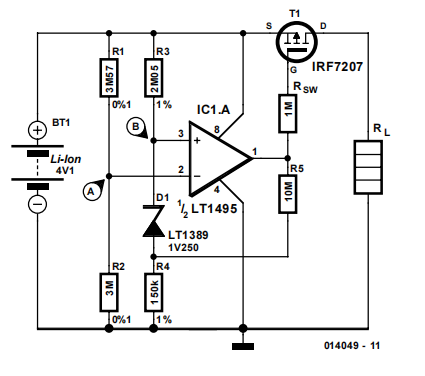
When a lithium-ion battery is discharged below the minimum recommended cell voltage its life expectancy is dramatically reduced. The circuit described here can avoid this by disconnecting the load from the battery when the cell voltage reaches a set level.The voltage at junction A may be set to 3 V, for example, by selecting the correct ratio of R1 and R2. When the battery voltage drops below the minimum value, the voltage at junction A will be smaller than that at junction B. The latter voltage is equal to: 

VB = 1.25 V + I R4 = 1.37 V

where:

I = (Vmin. – 1.25 V) / (R3 + R4) = 800 nA
(Vmin. = minimum value)

At this point the output of opamp LT1495 will go high, causing SW1 (a P-channel logic level MOSFET) to block and break the connection between the battery and the load. Because the battery voltage will rise when the load is disconnected, a certain amount of hysteresis is created by the addition of R5. This prevents the circuit from oscillating around the switching point. The value of R5 shown here provides 92 mV of hysteresis. So the battery voltage has to
rise to 3.092 V before the load is reconnected to the battery. An increase or decrease of the hysteresis is possible by reducing or increasing the value of R5, respectively. The required hysteresis depends in the internal impedance of the battery and the magnitude of the load current. The switching point defined by the values of R1-R2 is
quite critical with a circuit such as this. If the switching point is too high, then the available capacity of the battery is not fully utilised. Conversely, if the switching point is too low, the battery will be discharged too far with all the harmful consequences that may entail. Using the values shown here and including the tolerances of the parts, the switching point is between 2.988 V and 3.012 V. In practice it may be easier to select slightly lower values for R1 or R2 and connect a multi-turn trimpot in series with it. This makes an accurate adjustment of the switching point possible and has the additional advantage that R1 and R2 may be ordinary 1%-tolerance types.

Finally, before using the protection circuit it is advisable to first connect it to a power supply instead of a battery and carefully verify the operation of all its features!

Mains Powered


Many circuits can be powered directly from the mains with the aid of a series capacitor (C1). The disadvantage of this approach is that usually only one half cycle of the mains wave form can be used to produce a DC voltage. An obvious solution is to use a bridge rectifier to perform full-wave rectification, which increases the amount of current that can be supplied and allows the filter capacitor to be smaller. The accompanying circuit in fact does this, but in a clever manner that uses fewer components. Here we take advantage of the fact that a Zener diode is also a normal diode that conducts current in the forward direction. During one half wave, the current flows via D1 through the load and back via D4, while during the other half wave it flows via D3 and D2. Bear in mind that with this circuit (and with the bridge rectifier version), the zero voltage reference of the DC voltage is not directly connected to the neutral line of the 230-V circuit. This means that it is usually not possible to use this sort of supply to drive a triac, which normally needs such a connection. However, circuits that employ relays can benefit from full-wave rectification.

The value of the supply voltage depends on the specifications of the Zener diodes that are used, which can be freely chosen.
C2 must be able to handle at least this voltage. The amount of current that can be delivered depends on the capacitance of
C1. With the given value of 220 nF, the current is approximately 15 mA. A final warning: this sort of circuit is directly connected to
mains voltage, which can be lethal. You must never come in contact with this circuit! It is essential to house this circuit safely in a suitable enclosure.

source : Elektor Circuit Collections

Simple mV Source


This design can be used to simulate millivolt (mV) sensor signals for industrial control systems. Most of the new sensors used to day include some form of ‘intelligence’ at the measurement head, that is, the point at which the sensor comes into contact with what it is to measure. At this point, the sensor signal is conditioned/digitized and fed into a microcontroller that transmits a digital representation of the sensor value to the remote control system. However, there are still a number of ‘elderly’ control systems still in the field that have the intelligence remote from the sensor head. These systems rely on field wiring to convey the measured signal back to the control system.

During commissioning of these types of plant, it is useful to simulate the sensor signal to ensure amongst other things, that the sensor signal gets back to the correct terminals on the control system as they invariably pass through various junction boxes on the way. It can also be used to ensure that the control system operates correctly in response to the sensor signal. The design shown here has been used by the author to ‘bench test’ a control system prior to being installed. Please note that the design is only suitable for simple simulation and is not accurate enough for calibration purposes. Power from a ‘plugtop’ PSU (when bench testing) or a battery is fed to three current sources (diodes). Of these, I1 generates a 1.00 mA current signal, which when switched across the 100-Ω pot creates a 100-mV signal. Likewise, I2 generates a 0.25-mA signal which generates 25 mV across the pot. Current source I3 develops 3.0 mA and is used to illuminate the LED to give a power indication. The selected current source is switched via S2 to the 10-turn pot. Switch S1 is used to cleverly swap the polarity of the output signal. If the Type MTA206PA DPDT switch from Knitter is used, you get a centre-off position which actually shorts out the output signals (S1 pins 2 and 5) together, ensuring a zero output signal.

The current sources, despite being pretty expensive, are not very accurate — they have 10% tolerance! (hence the unsuitability for calibration use). If the output is too high, the tolerance can be ‘trimmed’ by fitting a bleed resistor (R1, R2) as shown in the diagram. The current sources are manufactured by Vishay/Siliconix and stocked by Farnell. The circuit draws a current of about 4.25 mA.

Measuring Inductors


Often you find yourself in the position of needing to wind your own coil for a project, or maybe you come across an unmarked coil in the junkbox. How can you best find out its inductance? An oscilloscope is all you need. Construct a resonant circuit using the coil and a capacitor and connect it to a square wave generator (often part of the oscilloscope itself) Adjust the generator until you find the resonant frequency f. When C is known (1000 pF) the inductance L may be calculated from:

L = 1 / (4Ï€2f2C)

If you are also interested how good the coil is i.e. what is its quality factor or Q, you can use the oscilloscope again. If the level of the damped oscillation drops to 0.37 (= 1/e) of the maximum after about 30 periods, then the Q factor of the coil is about 30

The Q factor should be measured at the intended operating frequency of the coil and with its intended capacitor. The coupling capacitor should by comparison be a much smaller value.

source : Elektor Circuit Collections 

Two Position Dimmer


This super-simple dimmer consists of only two components, and it can easily be built into a mains switch. If you do this, don’t forget to first switch off the associated branch circuit in the fuse box, since the mains voltage is always dangerous! The circuit does not need much explanation. When S1 is closed, the lamp works at full strength, and the position of S2 does not matter. When S1 is open and S2 is closed, the capacitor causes a voltage drop, so the lamp is dimmed. The power dissipation of the capacitor is practically zero, so the circuit does not generate any heat. The resistor prevents sparking when S2 is closed while S1 is already closed. The value of the capacitor can be matched to the power of the lamp to be dimmed; it should be between 2 and 6 µF. Be sure to use a class X2 capacitor. Also, don’t forget that thiscircuit works only with resistive (non-inductive) loads. Unpredictable things can happen with an inductive load!

source : Elektor Circuit Collections 2000-2014


±5-V Voltage Converter

A symmetrical ±5 V power supply is often needed for small, battery-operated operational amplifier projects and analogue circuits. An IC that can easily be used for this purpose is the National Semiconductor LM 2685. It contains a switched capacitor voltage doubler followed by a 5-V regulator. A voltage inverter integrated into the same IC, which also uses the switched-capacitor technique, runs from this output voltage. The external circuitry is limited to two pump capacitors and three electrolytic storage capacitors.

The IC can work with an input voltage between +2.85 V and +6.5 V, which makes it well suited for battery-operated equipment. The input voltage is first applied to a voltage doubler operating at 130 kHz. The external capacitor for this is  connected to pins 13 and 14. The output voltage of this doubler is filtered by capacitor C3, which is connected to pin 12. If the input voltage lies between +5.4 and +6.5 V, the voltage doubler switches off and passes the input voltage directly through to the following +5-V low-dropout regulator, which can deliver up to 50 mA. C4 is used as the output filter capacitor.

All that is necessary to generate the –5-V output voltage is to invert the +5-V voltage. This is done by a clocked power-MOS circuit that first charges capacitor C2, which is connected between pins 8 and 9, and then reverses its polarity. This chopped voltage must be filtered by C5 at the output. The unregulated –5 V output can supply up to 15 mA. The LM 2865 voltage converter IC also has a chip-enable input (CE) and two control inputs, SDP (shut down positive) and SDN (shut down negative). If CE is set Low, the entire IC is switched off (shut down), and its current consumption drops to typically 6 µA. The CE input can thus be used to switch the connected circuit on or off, without having to disconnect the battery. The SDP and SDN inputs can be used to switch the VPSW and VNSW outputs, respectively. These two pins are connected to the voltage outputs via two low-resistance CMOS switches. This allows the negative output to be separately switched off, whereby the voltage inverter is also switched off. Switching off with SDP not only opens the output switch but also stops the oscillator. There is thus no longer any input voltage for the –5 V inverter, so the –5 V output also drops out. The SDP and SDN inputs are set Low (< 0.8 V) for normal operation and High (>2.4 V) for switching off the associated voltage(s).

source : Elektor Circuit Collections 2000-2014


*SCAP' AVR Programmer

 By Michael Gaus (Germany)

Many newcomers to AVR programming would love to build their own low-cost programming device, but they face a chicken-and-egg problem: many of the designs themselves use an AVR microcontroller; this needs to be programmed, and so they first need to make a programmer...

This is where the SCAP (Serial Cheap AVR Programmer) can come in handy. It is a very simple programming device using a minimum of components, and it can be connected either directly to a PC's RS-232 interface or to a USB interface via a USB-to-RS232 converter.

The circuit includes a nine-way D-sub socket (K1) which can be connected to the PC's serial port or to the USB-to-RS232 converter. The circuit takes advantage of the internal protection diodes on the AVR's I/O pins to V cc and GND, and the two series resistors R1 and R2 are thus needed to limit the current flowing through these diodes. The values are chosen to keep this current below 1 mA. The RS-232 interface can be as high as ±15 V. At -15 V the AVR's internal protection diode to GND limits the voltage on the I/O pin to a minimum value of -0.7 V, while at +15 Vthe protection diode to V cc limits the pin voltage to a maximum value of V cc +0.7 V. Now, because the values of the series resistors R1 and R2 are relatively high, the charging and discharging of the AVR's input capacitance is considerably slower than if it had been driven directly by a push-pull stage, and this limits the maximum permissible frequency on SCK for reliable operation. The wiring of K2 corresponds to the standard six-way Atmel ISP connector.

The well-known open source program AVRDUDE is an essentially universal programming tool that can very easily be configured to work with SCAP: see [1] and [2]. The configuration file avrdude.conf needs to have the following section added to it:

This adds a new programmer called 'scap', which can then be selected as the device to be used for programming using the command-line option '-c scap'.

Even though the reset pin of the microcontroller is tied permanently to GND in the circuit, it must still be defined for AVRDUDE. If AVRDUDE fails to establish a connection with the AVR device to be programmed, the power to the device must be interrupted briefly to cause it to perform a power-on reset. Here is a sample command to invoke AVRDUDE. We have assumed that SCAP is connected to COM1 with an ATmega8 as the taret device (this corresponds to the commandline option '-p m8') and thatthe hex file to be programmed istest.hex.


avrdude 300 -


-P coml -p m8 -c scap U f lash : w : test . hex : i


The instruction to slow down SCK is specified by the command-line option '-i 300', which gives a delay of 300 jlls. This makes the programming operation rather slow. Depending on the type of interface used (normal RS-232 or a USB-to-RS-232 converter) it may be possible to reduce the delay value to as little as 50, which will make programming faster. If SCAP is being used just to solve the chicken-andegg problem mentioned at the start of this article, then programming speed will not be of any great concern

Internet Links

[1] AVRDUDE:

www.nongnu.org/avrdude/

[2] AVRDUDE version for Windows: www.mikrocontroller.net/ attachment/69851 /avrdude-5.1 0.zip

Power Controller for Convector Heaters


In Fall or Spring, the weather may be warm enough that we'd like to save money by shutting down the main heating system in our home and just use supplementary heating based on one or more electric convector heaters.

Even though these convectors are quite heavy consumers of electricity, this can be reduced by fitting a power controller between the heaters and the AC power outlet, which will affect the effective power consumption of the convectors.

The circuit diagram is based around the use of the emblematic NE555 IC, used here as an astable multivibrator with variable duty cycle (D = t high / T), but at a fixed operating frequency, given by:

f = 1 / (0.693 x PI x C6) = 0.0654 Hz

The duty cycle D of the signal at the output (pin 3) of IC2 will change depending on the position of the wiper of potentiometer PI :

• If the wiper is at mid-travel, the duty cycle D will be 0.5;

• If the wiper is at the +12 V end, the IC2 output signal is zero and hence D = 0;

• If the wiper position takes it down to the voltage on C6, IC2's output supplies a constant voltage of around 11 V and D = 1.

By way of transistor T1, IC2 drives two MOC3021 phototriacs (IC3 & IC4) which provide the isolation between the circuit's 'driver' section and the 'power' section, which is directly connected to the AC powerlines.

Each phototriac drives a power triac (TRI1 & TRI2). These two triacs are fitted in parallel and share the task of supplying the convector (R L ): one triac supplies the positive half-cycle while the other triac supplies the negative

A Few DC Solid-state Relays

 By Georges Treels (France) (Elektor Electronics)

Good old electromechanical relays are relatively expensive where any significant current has to be switched and switching times must be short. One solution is to go over to solidstate relays (SSRs). In DC mode, MOSFETs offer a very interesting solution, and the various manufacturers today offer devices at less than £4 with amazing performance, in terms of both current and low R DS ( on y They're relatively simple to use, in both monostable and bistable modes, so why stint ourselves?


The following circuits will let you switch 10-60 A (or even more if you use configurations with MOSFETs in parallel), with very short switching times. Several configurations are shown, monostable and bistable, capable of switching a load with one side returned to either ground (high side switching) or the positive rail (low side switching). In addition, the monostable configurations offer galvanic isolation and can be driven by signals from 5-24 V, DC or AC. The bistable SSRs are controlled using a simple push-button and a little bit of logic.


Let's start with the monostable SSRs. Bridge B1 makes it possible to accept any input polarity in the case of a DC control signal, and rectifies the signal in the case of an AC control signal. The network R1, R2, D1 limits the LED current in opto-isolator IC1 . The base of the phototransistor in IC1 is connected to ground via R3; its emitter is connected directly to ground.


In the case of a load returned to ground, the gate of T1, a P-channel MOSFET, is driven directly from the collector of IC1. If the load is returned to the positive rail, the gate of T1, this time an N-channel MOSFET, is driven via T2, which inverts the output from IC1 .


C2, C3, D2, and D3 protect the MOSFET in the event of loads that are not purely resistive. Both bistable configurations use the same power stages as the monostables, with an N-MOSFET for loads connected to the positive rail and a P-MOSFETfor loads connected to ground.


IC1.A is wired as a simple flip-flop: with the switching threshold set by PI , IC1 .A output will change state each time button SI is pressed. R1 and CI avoid rapid oscillations while SI is pressed. IC1 gates B, C, and D directly drive the gate of the P-MOSFET in the case of a load returned to ground. IC1 .B inverts IC1 .A output when an N-MOSFET has to be driven (load returned to the positive rail). In both configurations, the relay remains off at power-on (safety feature).


Concerning the MOSFETs, the table lists a number of possible types. This list is far from being exhaustive and new devices come out regularly. Give preference to a low value of R DS(on) (dissipation) and a good dv/dt specification in the case of 'dirty' loads. Pay attention also to the V DS . Even though most of these transistors can take 60 V, this is not the case for either the optoisolators or the bipolar transistors used.

If you are designing a PCB for this type of relay, pay attention to the possibility of heavy currents being carried by the PCB track. For example, three SUP75P03-07 wired in parallel can pass over 200 A! Bear in mind that a PCB track with a copper layer 35 jam thick (i.e. standard) has a resistance of 48* 10 5 x L/ Wohms, where L(ength) and W(idth) are in mm.


Wideband PC Radio


PC radios are certainly nothing unusual. However, unless you are prepared to spend a lot of cash you can't buy a wideband PC radio that receives short-wave signals — if you want one that will not break the bank, you will have to build it yourself. There's no need for a battery or power supply, since power can be drawn directly from the PC serial interface. The audio signal is fed into the PC sound card. The circuit diagram in Figure 1 shows this simple audion receiver. The transistor in the common-emitter circuit demodulates AM signals, thanks to its exponential characteristic curve. Since the base-emitter junction is already biased, RF potentials of a few millivolts are sufficient to achieve demodulation. For this reason, the audion circuit is significantly more sensitive than a simple diode detector.


So where is the tuning capacitor? It's not needed, since the receiver has an extremely wide bandwidth and (simultaneously!) receives all strong signals ranging from the 49-m band to the 19-m band. The coil is wound in two layers with 15 turns on a pencil. This yields an inductance of around 2 uH. The resonant circuit capacitance of around 100 pF is composed of the base capacitance of the transistor and the aerial capacitance. This places the resonant frequency at around 11 M Hz. The low input impedance of the transistor damps the resonant circuitto the pointthat its Q factor is 1, so the bandwidth is also around 11 M Hz. The receiver thus picks up everything between 6 MHz and 17 MHz. This complete elimination of the usual selection leads to surprising results.


Less is more. For communications technicians, this means: less selectivity = more bandwidth = more information. Indeed, here you dive into a sea of waves and tones. The special propagation conditions for short-wave signals cause first one signal and then another signal to predominate. You hear messages in several languages atthe same time, music ranging from classical to pop and folk songs from distant countries. Without the bother of the usual dial spinning, you can roam at your leisure through the entire short-wave region.


The supply voltage for the radio must be first switched on by using a program (HyperTerminal is adequate) to switch the DTR lead of the serial interface from -10 V to +10 V. If you want to avoid this trouble, you can use a PNP transistor. The alternative circuit diagram shown in Figure 2 shows some additional improvements. The coupling capacitor prevents the dc component from reaching the input of the sound card, and residual HF components are shorted out by the parallel capacitor. With these modifications, the radio is also quite suitable for direct connection to a stereo system, final amplifier or active speaker. In such cases, you can do without the PC and use a battery (1.5 to 12 V) instead. A downpipe from the eavestrough can be used as an aerial if it is insulated at its lower end (where it connects to the sewer system) by a rubber ring or concrete. If you are not so fortunate as to have access to such an arrangement, you will have to rig a wire aerial (at least 5 m long).

source : Elektor Circuit Collections 


Pressure Switch


A simple pressure switch with a range of 50 to 350 mbar can be made using a pressure sensor. If you can accept somewhat reduced linearity, the sensor can even be used up to 500 mbar. As shown in the schematic diagram, the circuit contains very few components other than the sensor. Dl, Rl, CI and D5 form a simple voltage stabiliser that holds the supply voltage for the sensor and opamps at 5 V The three diodes in series with the sensor provide temperature compensation (more on this later). The differential output signal from the sensor is amplified 30 x by an instrumentation amplifier composed of opamps ICla, IClb and IClc. 


The amplification factor can be adjusted if necessary by modifying the value of R10. The amplified output signal is compared to the voltage on the wiper of PI. If the voltage that results from the pressure being measured is less than the value set by PI, the output of comparator ICld is High and LED D4 is on. An external load can be switched via the open-collector output of T2. 

We used a Melexis MLX90240 sensor (www.melexis.com), but unless you work in the automotive industry, you won't be able to obtain this sensor. An Exar sensor (such as the SM5310-005-G-P; see www.exar.com) or a Motorola type can be used instead. If necessary, the circuit can bemodified as described below. Start with the sensor sensitivity specification from the data sheet (approximately 60 mV/bar/volt in our case). Since the supply voltage of the sensor is 5 V minus 3 diode drops, or around 3 V, the net sensitivity is thus 180 mV/bar. 

The range of the sensor is 0 to 350 mbar, so the maximum output voltage is 63 mV. The following amplifier has a gain of approximately 30, so the output signal ranges between 0 and 1.89 V. This voltage is compared to the voltage on the wiper of PI, which can be varied between 0 and 2.5 V. If the sensitivity differs from the nominal value, the amplification can be adjusted as necessary using R10. 

Finally, a remark on the temperature compensation. The sensor used here has a temperature coefficient of 2100 ppm/degree. 

Other types of sensor will have somewhat different values (consult the data sheet). The supply voltage should thus increase by 2100 ppm of 3 V for every degree, which is 6.3 mV per degree. The voltage across a silicon diode drops approximately 2 mV per degree, so the supply voltage of the sensor increases as the temperature increases. This compensates for its decreased sensitivity. With the indicated sensor, three diodes in series are needed to just about fully compensate for its temperature coefficient. Two diodes are sufficient for the previously mentioned Exar sensor.

PC Battery Charger

 Some workbenches can't help ending up looking like a rats nest of cables and equipment, so its always an advantage if a piece of mains equipment can be removed from somewhere to free up an extra mains socket. Here we are using the ubiquitous PC as a battery charger. An unused serial interface port can supply enough current to charge (or trickle charge) lowcapacity Nickel Cadmium (NiCd) batteries. You could for example, use the batteries in a radio and charge them during use.

The three serial port connections TxD, DTR, and RTS, when not in use, are at -10 V and can supply a current of around 10 to 20 mA (they are short-circuit protected). The circuit shown supplies a charging current of approximately 30 mA. If it is necessary to alter the polarity of the charging circuit then it is a simple job to reverse the diodes and using software, switch the port signals +10 V. Those interested could also write a software routine to automatically recharge the batteries.