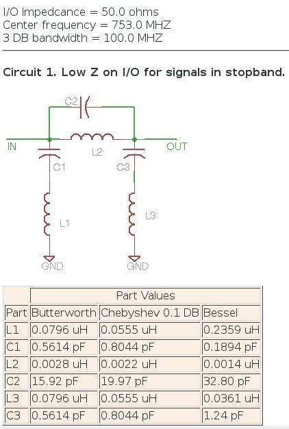
LM 335 Temperature Sensor Circuit

Temperature Control Circuit :

Image Courtesy Texas Instrument


The temperature controller circuit using +5 V voltage source from I/O slot at IBM PC/XT/AT.

IC LM 335 from Texas Instrument have the ability to detect temperature from ranging -40 celcius degree until 100 celcius degree.
This LM 335 from Texas Instrument , is zener diode which have the linear coefficient voltage increment related with increment of temperature with formula :

Vz = + 10 mV/ C (celcius degree) , with current opeartion between 400 uA until 5 mA.

On the circuit Resistor 2.2 K use for limit the current flow to cathode pin from LM 335 which is output of LM 335 sensor temperature.
On circuit Resistance of R is 2.2 K , and at 25 Celcius degree from data sheet of LM 335 , voltage at LM 335 will be 2.982 Volt , so current flow can be calculate :

Vcc = + 5 V
Voltage at 25 Celcius on LM 335 = 2.982 V
Voltage at Resistor R 2.2K is = 2.018 V
Current flow through LM 335 and R will be = 2.018 V / 2.2 K = 0.9 mA

This 0.9 mA current at LM 335 still on at range of sensor LM 335, and then the output cathode pin of LM 335 sensor from Texas Instrument connect to input 0 of ADC0809 Analog and Digital convertion data from Texas Instrument at pin 26.

Temperature Sensor LM 335 from Texas Instrument


Temperature Sensor using IC LM 335 from Texas Instrument. LM 335 is Zener Diode which sensitive of temperature change in it surrounding , which is reverse bias on it breakdown area with output :

Vz = [10 mV/Kelvin] …..........[2-1]

Because there is gap different 273 degree between Kelvin and Celcius , so the output in Celcius for LM 335 from Texas Instrument will be :

Vz = 2.73 Volt + [ 10 mV/Celcius] T.........[2-2]

where T is in Celcius Degree

IC LM 335 from Texas Instrument have temperature range between -40 celcius degree – 100 celcius degree

I use LM 335 in Plastic Package TO-92 , another package for LM 335 is SOIC 


Images courtesy Texas Instrument

Another IC temperature sensors from Texas Instrument are LM135, LM135A with TO-46 package, LM235 and LM235A in TO-92 package and LM 335 and LM 335A in SOIC package.

From this writing, I want to discuss about Simulation control system with IBM PC 
XT/AT for Temperature, heater, and pump using LM 335 as sensor, PIO 8255, ADC 0809 , MOC  from motorolla , and TRIAC .
This control system operate with software with QBasic , and I will write the schematic diagram, implementation, and software design.

For more data about LM335/LM335A . please visit data from Texas Instrument , here

4G LTE Bandstop Antenna UHF Filter 703 MHz - 803 MHz

As from 4G LTE Band spectrum, we can see that at LTE Band 44 , allocation frequency of 4G LTE at 703 MHz-803 MHz. And this spectrum frequency , overlapping with digital TV spectrum. As we know, digital tv spectrum frequency at band 703 MHz - 803 MHz, with bandwith 100 MHz.
So the center frequency will be :

Center Frequency 703 - 803 MHz = 753 MHz

I use Bandstop filter calculator refer to http://www.wa4dsy.net/filter/filterdesign.html

 After we input the parameter of center frequency 753 MHz , and bandwith 100 MHz at calculator, then click compute parts as the menu on calculator, then we get the result of 3 filter design with 2 circuit , butterworth, bessel, and chebyshev.


The component values of  3 design filter, for butterworth, bessel, and chebyshev are :
 You can choose one of three offering design and choose one of two circuit for your implementation.
The output chart graph of filter design are :


3 Pole Bandpass Filter for uhf digital tv 470-800 MHz


This 3 pole bandpass filter using https://wetnet.net/rf_design/3pole.main.cgi  design calculator online.
this bandpass filter is butterworth filter and intended to filter digital tv bandwith 470MHz to 800 MHz , and only this signal will detected after antenna.
Parameter of filter :
Band Frequency 470 - 800 MHz
Center Frequency = 635 MHz
Bandwith = 400 MHz
Impedance = 50 ohm

Input this parameter to online filter calculator above :

 Click Submit , and the result :


L1,L3 : 0.008763 uH ( 8,763 nH)
L2      : 0.039789 uH (39.789nH)

C1,C3 : 0,000008 uF ( 8 pF)
C2      : 0,000001753 uF (1,753 pF)

We must determine for Inductor L1,L2,L3 the coil diameter, coil length and number of turn of coil.
Using online calculator from  http://www.qsl.net/in3otd/indcalc.html we can determine diameter, length and number of turn coil.
For L1,L3 :

L = 0,00876 uH , coil diameter will be  d : 0,01 m  , Coil length will be l  : 0.01 m and number of turns , n : 1,1355

And for L2 :

L = 0,0396 uH , coil diameter will be d : 0,0259 m , coil length will be l : 0,01 m and number of turns n : 1,1355

The most important thing of build filter is the connection between component should be as close as possible, for avoiding wild capacitance that will generate noise, and the ground area of PCB should be good and wide.
On the next article, I will posting the implementation of this filter.

LSI Chip intel Programmable Peripheral Interface (PPI) 8255

Intel Chip PPI 8255


Image courtesy of wikipedia.org

Chip LSI internal configuration PPI 8255 shows the figure 1. In figure 1, pin IC 8255 consists of 3 groups:
1. Read / Write Control Logic
2. Data Bus Buffer
3. Input / Output Ports

Image courtesy of wikipedia.org


READ / WRITE CONTROL LOGIC

Groups Read / Write Control Logic organize all data and controls, both internal transfers Form and Form of Transfer externally. ACCEPT singer group input from address bus and bus control CPU, the group later realize Ke - Control group. Pin - pin Of The Read / Write Control Logic is as follows:

CS (Chip Select)

Low ON signal pin singer will be to enable communication LSI Chip PPI BETWEEN 8255 TO microcomputers.

RD (Read):
Low ON signal pin singer will be to enable the CPU to review read status information OR Data From Chip LSI PPI 8255

WR (Write)
Low ON signal pin singer will be to enable the CPU to write a review OR Data Into PPI control word 8255
A0 and A1:
The input selector is functioning as part of the Joint Control word - the same WITH RD and WR. Basic Operations The Group is controlled by the Read / Write Control Logic singer portrayed ON the table below.

re:
ON logic high reset input will be to clear the contents of the list of controls and harbor ALL To set the input mode.

Control Group A and Group B:

Configuration functions From EVERY port in the software program by. IN AN basically CPU provides output control word addressed to the LSI Chip Control Word 8255. PPI mode provides information about, bit set, bit reset, And Others. Singer configuration is used to initialize the configuration functions review Chip LSI 8255 PPI.

EVERY Control blocks (Group A and Group B) RECEIVE command From the Read / Write Control Logic, And said menerimacontrol Data From internal bus (internal data bus) and execute commands - Commands Right to review arrangements port - port ITU. ON said control registers can only perform write operations, NO can perform read operations.

DATA BUS BUFFER
The data bus is a 3 state buffer 8 bit With operations Operating prayer Arah (both directions), ayng used to review 8255 WITH connect Chip PPI data bus system. Data Sent and received through the data buffer bus, Similarly to review the control word.

PORT INPUT / Output
Port Input / Output Was Part Of The 8255 PPI chip serves as a liaison