Antenna Handbook

Simple RF Detector for 2 m

This simple circuit helps you sniff out RF radiation leaking from your transmitter, improper joints, a broken cable or equipment with poor RF shielding. The tester is designed for the 2-m amateur radio band (144-146 MHz in Europe).

The instrument has a 4-step LED readout and an audible alarm for high radiation voltages. The RF signal is picked up by an antenna and made to resonate by CI -LI. After rectifying by diode Dl, the signal is fed to a two-transistor highgain Darlington amplifier, T2T3. Assuming that a 10-inch telescopic antenna is used, the RF level scale set up for the LEDs is as follows:


When all LEDs light, the (optional) UM66 sound/melody generator chip (IC1) is also actuated and supplies an audible alarm. By changing the values of zener diodes D2, D4, D6 and D8, the step size

and span of the instrument may be changed as required. For operation in other ham or PMR bands, simply change the resonant network CI -LI.

As an example, a 5-watt handheld transceiver fitted with a half-wave telescopic antenna (G = 3.5 dBd), will produce an ERP (effective radiated power) of almost 10 watts and an e.m.f. of more than 8 volts close to your head.


Inductor LI consists of 2.5 turns of 20 SWG (approx. 1 mm dia) enamelled copper wire. The inside diameter is about 7 mm and no core is used. The associated trimmer capacitor CI is tuned for the highest number of LEDs to light at a relatively low fleldstrength put up by a 2-m transceiver transmitting at 145 MHz.

The tester is powered by a 9-V battery and draws about 15 mA when all LEDs are on. It should be enclosed in a metal case.

Noise Injector


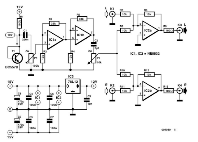
This Circuit is primarily intended to be used by persons who want to experiment with audio. For example, you can determine whether your own audible threshold for noise is different with and without music, or whether a particular CD sounds better with a little bit of noise. However, since this circuit produces white noise, it can also be used for test measurements, such as comparing the sounds of different loudspeakers, measuring filter characteristics and so on. The measured characteristics, as shown in Figure 2, show a nearly flat amplitude distribution (averaged over 64 measurements). The effective value of the noise signal at the output is around 100 mV maximum (with both potentiometers set to maximum), measured over the frequency range of 22 Hz to 22 kHz.

The noise is generated by reverse-biasing the base-emitter junction of a PNP transistor (BC557B) so that it zeners. In our prototype, the voltage across Tl was approximately 10 V. PI is used to set the level of the generated noise so that it is just audible, following which the output level can be adjusted using the logarithmic potentiometer P2. For making measurements, PI can also be simply set to its maximum position. The noise is amplified by two opamp stages. Depending on the transistor manufacturer, or the type of transistor if you use a different type, the level of the generated noise can vary significantly. Using two amplification stages in series provides more options and considerably more bandwidth, and you can implement various filter characteristics around ICla and IClb according to your own taste. The gain of the two stages has been kept equal to ensure the maximum possible bandwidth. The amplified signal is then passed to a simple summing amplifier (IC2). We have used a stereo arrangement, in which both channels receive the same noise signal. If you want to expand on the design, you can provide each channel with its own noise generator. In this case, you will have to use a dual potentiometer for P2.

The well-known NE5532 is used for the amplifiers, but any other good dual opamp would also be satisfactory. The opamps are fed from a standard, symmetrical ±15-V supply. In order to suppress possible positive feedback via the power supply, and to reduce the effects of power supply noise (since the opamps are non-inverting), the supply for the noise diode circuit (Rl and Tl) is separately stabilised by IC3 (7812) and extra filtering for the ± 15-V supply is provided by C8 and C9. IC3 must be located as close as possible to Rl, Tl and IC1. The coupling capacitors CI and C2 are necessary to prevent the DC component of the noise signal from appearing at the outputs.

The table lists some measured characteristics of the circuit, for a bandwidth B of 22 Hz to 22 kHz and a reference level of 2V eff .


NE555 Datasheet

The LM555/NE555/SA555 is a highly stable controller capable of producing accurate timing pulses. With a monostable operation, the time delay is controlled by one external resistor and one capacitor. With an astable operation, the frequency and duty cycle are accurately controlled by two external resistors and one capacitor


Features :

• High Current Drive Capability (200mA) 

• Adjustable Duty Cycle 

• Temperature Stability of 0.005%/°C 

• Timing From µSec to Hours 

• Turn off Time Less Than 2µSec 


Applications :

 • Precision Timing 

• Pulse Generation

 • Time Delay Generation 

• Sequential Timing 

Simple Touch Pad Dimmer


Using a Power-FET it is possible to build a very simple touch dimmer for low voltage lamps. Two drawing pins are used here as the touch contacts. The electrical resistance of your skin is in the order of 100 kQ to 1 MQ. The circuit operates as an integrator with a capacitor in its negative feedback path. This configuration gives a relatively linear control character¬ istic. Once you have selected a brightness level, it will be maintained for hours if you use a low leakage (foil) capacitor. Another feature of this circuit is that the harder you press on the contacts, the quicker the lamp brightness changes.

Low-Noise Microphone Amplifier


The signal from a microphone is two weak for a standard line input. This low-noise DC-coupled microphone amplifier pro¬ vides a solution for anyone who wants to connect a micro¬ phone to his or her hi-fi installation. As can be seen from the schematic diagram, a good circuit does not have to be com¬ plex. A differential amplifier is built around T1 (MAT-03E), which is a low-noise dual transistor. The combination of T2 and LED D1 forms a constant-current source for the input stage. A low-noise opamp (OP-270E) amplifies the difference signal that appears at the collectors of the dual transistor. The result is an analogue signal at line level. The bandwidth of the amplifier ranges from 1 Hz to 20 kHz. Within the audio range (20 Hz to 20 kHz), the distortion is less than 0.005 percent. Since only half of the OP-270E is used, the remaining opamp could be used in the output stage of a stereo version.


The amplifier can be powered from a stabilised, symmetrical supply with a voltage between ±12 V and ±15 V. Such sup¬ ply voltages are already present in many amplifiers.